


Image Gallery
19 Electrons Trapped In A Spherical Electric Field

19 electrons trapped in a spherical electric field. They form shells like atoms in the periodic table (notice the symmetry), and they may "freeze," i.e. crystallize like in this figure. Phys. Rev. Focus (2001).

A ~120 Angstrom Square Region

An image of a ~120 angstrom square region of the BiO surface of the high Tc superconductor Bi-2212.
A Current Image Is Taken At 50meV In The Twin Domain Boundary Of Underdoped Ca(Fe1-xCox)2As2

A current image is taken at 50meV in the twin domain boundary of underdoped Ca(Fe1-xCox)2As2. The static unidirectional electronic structures change directionality by 90 degrees across the twin boundary. The autocorrelations of the respective domains are shown in the insets; center of self-similarity peaks (gray lines) are separated by ~8aFe-Fe. T.-M. Chuang, M. P. Allan, Jinho Lee, Yang Xie, Ni Ni, S. L. Bud'ko, G. S. Boebinger, P. C. Canfield, J. C. Davis. Science 327, 181 (2010).
A Hexatic Membrane With Its Characteristic Dislocations

A snapshot of a hexatic membrane with its characteristic dislocations (yellow-blue dimers). Any sufficiently flexible elastic membrane with finite bond energies will melt via the formation of such dislocations to create a fluctuating analog of a bond-orientationally ordered planar hexatic. Mark Bowick, Chapter 11 in "Statistical mechanics of Membranes and Surfaces," ed. by D.R. Nelson, T. Piran, and S. Weinberg (World Scientific, Singapore, 2004).
A Human Hair Into Which the Logo Of the Center for Nanointegration Duisburg-Essen (CeNIDE)

A human hair into which the logo of the Center for Nanointegration Duisburg-Essen (CeNIDE) was engraved using a focused ion beam (FIB).
A Model Of The Spin-Triplet

A model of the spin-triplet, organic superconductor (TMTSF)2PF6.
A Post-Rendered Image Of The Variations In The Electronic Cluster Glass (ECG) In Underdoped Na-CCOC

A Post-Rendered Image Of The Variations In The Electronic Cluster Glass (ECG) In Underdoped Na-CCOC.J.C. Seamus Davis, Cornell University; H. Takagi, RIKEN, University of Tokyo, and S. Uchida, University of Tokyo. Cover Article: Science 315, 5817 (2007).
A Schrödinger's Cat State

A Schrödinger's cat state is detected in superconducting nanowires at high bias currents through the analysis of the statistics of the switching currents. It is demonstrated that at high bias currents the entire number of superconducting electrons in an ultrathin superconducting wire can quantum-mechanically tunnel from a state having a higher electrical current to one having a lower current. Since the effect involves a large number of electrons it is called macroscopic quantum tunneling (MQT). Another term used to describe such tunneling is "quantum phase slip" (QPS). Unlike in previous reports on superconducting nanowires, here the conclusion about the presence of QPS is reached by measuring and analyzing the fluctuation of the switching current at T=0.3 K. M. Sahu, M.-H. Bae, A. Rogachev, D. Pekker, T.-C. Wei, N. Shah, P. M. Goldbart and A. Bezryadin, Nature Physics 5, 503 (2009).
A Single-Walled Carbon Nanotube of 75 Nanometers

A single-walled carbon nanotube of 75 nanometers can stretch to 84 nanometers before it breaks. J. Y. Huang, S. Chen, Z. Q. Wang, K. Kempa, Y. M. Wang, S. H. Jo, G. Chen, M. S. Dresselhaus, Z. F. Ren. Nature 439, 281 (2006).
A Suspended Graphene Device

A suspended graphene device. Image courtesy: Dr. Yong P. Chen, Purdue University.
Atomic epitaxy-like interfacial self assembly of gold nanoparticle monolayers

These are optical microscopy images of gold nanoparticle islands that are nucleating and growing over time on the liquid-air interface of a drying drop. The ~6 nm gold nanoparticles are ligated with dodecanethiol and dissolved in toluene. They impinge on and stick to the liquid-air interface where they self-assemble to form highly crystalline monolayer domains, similar to atomic epitaxy. The first frame shows the interface before nucleation and growth. The second frame and onward shows nanoparticle islands growing on the interface (note that optical microscopy cannot resolve the monomers nor the island nuclei). In the final frame, islands coalesce to form a single continuous monolayer that eventually covers the entire surface of the drop. We are adapting atomic epitaxial growth models to model the nanoparticle self-assembly process and better understand the forces and dynamics that govern assembly. We will present results from this project at the APS March Meeting. Each frame is ~175 µm in width. (credit: C. P. Joshi, Y. Krukov, J. G. Amar, T. P. Bigioni)
Atomic Force Microscopy Image Of A Single Silicon Adatom

Atomic force microscopy image of a single silicon adatom, size 660 pm x 660 pm x 120 pm. The two crescents are interpreted to represent two orbitals originating in a single tip atom. Giessibl, Hembacher, Bielefeldt and Mannhart. Science 289, 422 (2000).
Boron Nitride Nanotubes

Boron nitride nanotubes are materials whose existence theorists predicted before they were synthesized in laboratories. The pictured image is a simulation of a single nanotube. This material has the intriguing property that the greatest density of conduction electrons is along the tube axis. Boron nitride nanotubes thus can ballistically conduct electrons down the center of the tube. Marvin L. Cohen, University of California, Berkeley. Physics Today 59 (6), 48 (2006). 2006, American Institute of Physics.
Carbon Nanotubes

An array of aligned, but randomly placed, carbon nanotubes which can act like a radio antenna for detecting light at visible wave-lengths. The scale bar is one micron in length. K. Kempa, Z. Ren et al., Appl. Phys. Lett. 85, 13 (2004).
Ceramic Superconductor Single Crystal

Characterization Of High-order Harmonics From Crystals

Self-referencing interferometry is utilized to characterize the dipole phase of high-order harmonics from crystals, J. Lu, E. Cunningham, Y.S You, D.A. Reis, and S. Ghimire, Nature Photonics, Dec 17, advance online, 2018, https://doi.org/10.1038/s41566-018-0326-x
Computed Flow Of Electrons Away From A Quantum Point Contact

Computed flow of electrons away from a quantum point contact in a two dimensional electron gas with small angle scattering. The potential which scatters electrons is shown, together with the calculated flow, which forms branches at distances less than the mean free path. Physics Today 56 (12) (2003).
Computer Simulation Of Electrical Conductivity Versus Magnetic Field Directions

Computer simulation of electrical conductivity versus magnetic field directions in the one-dimensional molecular organic conductor (TMTSF)2PF6. Red (blue) regions represent high (low) conductivity, showing angular magnetoresistance oscillations (AMRO) due to interference between electron waves at commensurate field orientations. This phenomenon is presently being investigated in micro- and nano-size crystals.
Edge Electron Dynamics in Irradiated Graphene Nanoribbon
An edge-state electron wave packet flows around a defect in a laser-irradiated graphene nanoribbon. When circularly-polarized light impinges on a zig-zag graphene nanoribbon (one dimensional graphene stripe), the material becomes a topological insulator. This means that electrons can perfectly move along its edges, flowing around defects and impurities unaffected, as this images obtained by theoretical simulations shows.
Electrically Detected Spin Readout Experiments

Electrically detected spin readout experiments. Conduction electrons (green) flow through a silicon chip and can only be trapped by phosphorus atoms with a different electron spin (blue). This spin-trap was used to measure the longest electrically-detected spin coherence: G. W. Morley et al., Phys. Rev. Lett. 101, 207602 (2008). The same experiment was also used to initialize the nuclear spins (red arrows) and to electrically readout their state after storing information therein for over 100 seconds. D. R. McCamey, J. van Tol, G. W. Morley & C. Boehme, Phys. Rev. Lett. 102, 027601 (2009), and D. R. McCamey, J. van Tol, G. W. Morley & C. Boehme, Science 330, 1652 (2010).
Electron Flow Away From A Quantum Point Contact

Scanned probe microscope images of electron flow away from a quantum point contact formed in a two dimensional electron gas inside a GaAs/AlGaAs heterostructure. Small angle scattering causes branches of electron flow to form at distances less than the mean free path. Robert Westervelt, Harvard University, Arthur C. Gossard, UC, Santa Barbara, Physics Today 56(12) (2003).
Electron-Spin Data

Spinscape: Electron-spin data from a spin-shifting microstructure shows variations from almost no spin (flat regions) to rapid spin (ridges) in a particular direction. Y. Kato, R. C. Myers, D. C. Driscoll, A. C. Gossard, J. Levy, D. D. Awschalom. Science News 163(8) (2003).
Electrons In A Two Dimensional Electron Gas

Scanned probe microscope image of electrons in a two dimensional electron gas inside a GaAs/AlGaAs heterostructure at a low temperature. A strong magnetic field produces the quantum Hall effect, and causes the patterns shown. Raymond Ashoori, MIT, Physics Today 56(12) (2003).
Epoxy-Carbonyl Combination of Graphene Oxides
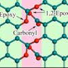
Top panel: prototypes of oxide functional groups on carbon. Middle and bottom panels: top and side view of the epoxy-carbonyl configuration, respectively. Pink color shows the region functionalized by oxygen.
Ge/Si Core/Shell Nanowire Heterostructures

Ge/Si core/shell nanowire heterostructures, when coupled to superconducting leads, are tunable mesoscopic Josephson junctions. The underlying plot is a map of the differential conductance as a function of both gate and source-drain voltage, with multiple Andreev reflections giving rise to the observed pattern.
Andy Vidan, MIT Lincoln Laboratory. Nature Nanotechnology 1, 208 (2006).
Graphene Films

Single atomic-layer graphene visible to bare eye. Left: A 4-inch monolayer graphene film grown by chemical vapor deposition (CVD) floating on an aqueous solution. Right: Two monolayer graphene films transferred to glass substrates. Such graphene films can be used as transparent electrodes. H. Cao et al., Appl. Phys. Lett. 96, 122106 (2010)
Ground States Of A Collection Of N Point-Like Particles

Ground states of a collection of N point-like particles constrained to lie on the surface of a torus and interacting via a cubic potential. The lattices are labeled by (r,N), where r is the ratio between the largest and smallest radius of the torus. The figure shows prominent example of topological defects such as dislcinations (5-fold disclinations are marked in red and 7-fold disclinations in blue), dislocations and grain-boundaries. While in planar crystals these defects are energetically costly and don't appear in the ground state, on a surface of non-zero Gaussian curvature defects proliferate in order to balance the elastic strain introduced by the curvature of the underlying medium. L. Giomi and M. J. Bowick, Eur. Phys. J. E 27, 275 (2008) & M. Bowick and L. Giomi, Adv. Phys. 58, 449 (2009).
How Doping Changes The Band Positions Relative to Fermi Level

An experimental demonstration of how doping changes the band positions relative to Fermi level, key to semiconductor device fabrication. This is the first direct demonstration of this effect in a polymeric semiconductor. Peter Dowben, Appl. Phys. Lett. 80, 4342 (2002).
Image Gallery Submissions
Landau spectrum in a bismuth single crystal

Landau spectrum in a bismuth single crystal obtained by measurements of angle-resolved Nernst effect at T=0.49 K. The magnetic field is tilted off the trigonal axis in the trigonal-bianry plane.
Lead Disulfide Microcrystals

Atomic force microscopy (AFM) image of lead disulfide microcrystals grown on a silicon oxide surface patterned by the AFM using "Dip-pen Nanolithography" (DPN). The field of view is 11.6 µm across, and the hexagonal crystallites are about 60 nm high. DPN was used to write a 5 µm x 5 µm chemically-reactive region on the wafer, which was then soaked in lead acetate and exposed to H2S gas. Microcrystals selectively grew starting from the patterned area. S. E. Kooi, L. A. Baker, P. E. Sheehan, and L. J. Whitman.
Light absorption by gold nanoparticle

The electromagnetic wave with a 500 nm wavelength is incident on a gold nanoparticle on a dielectric substrate. The figure shows the background electric field norm, for φ = π/4, θ = π/6 angles of incidence (left) and the norm of the total electric field for the same angles of incidence, after it has been influenced both by the material interface and by the gold nanoparticle (right). It is shown that the light absorption is increased by orders with the presence of the nanoparticle.
Low-Energy Wannier States (WS) Of Real Materials

Low-energy Wannier states (WS) of real materials. Top: Gapless excitations in the charge density wave phase of TaSe2 is explained with the unique geometric effects derived naturally from the phase interference of the WS. The hyrdization of 'ag and eg' symmetry essential to the understanding is clearly observed. (Phys. Rev. Lett. 96, 026406 (2006)). Bottom: Unexpectedly strong spin-dependence of resonant inelastic x-ray spectrum of LaMnO3 is explained by the strong charge transfer nature of LaMnO3, which is directly observable from the large hybridization with O-p states in the WS. Based on further novel WS analysis, origin of orbital ordering of MnF3 and LaMnO3 is, surprisingly, mainly electron-electron interaction, rather than the electron-phone coupling (Jahn-Teller effects). (Phys. Rev. Lett. 94, 047203 (2005) & cond-mat/0509075).
Nickel-Copper On Mica

One Jump, Or Avalanche, In Our Model For Crackling Noise In Magnets

One jump, or avalanche, in our model for crackling noise in magnets. The first spins to flip are colored blue, and the last pink. Notice the fractal structure: the avalanche is rough on all time scales. James P. Sethna, Karin A. Dahmen, Christopher R. Myers. Nature 410, 242-250 (2001).
Quasicrystals

Quasicrystals. Crystals are surely the oldest known of the broken-symmetry phases of matter, and remain the most beautiful illustrations. It's amazing that in the past few years, we've uncovered an entirely new class of crystals. Shown here is a photograph of a quasicrystalline metallic alloy, with icosahedral symmetry. Notice the five-pointed stars: our old notions of crystals had to be completely revised to include this type of symmetry. J. H. Lang, M. Audier, B. Dubost, and P. Sainfort, J. of Crystal Growth 83, 456 (1987).
Reflection Optical Microscope Image

Reflection optical microscope image of the dried suspension of lithographically defined 60-nm-thick, ~1 micron diameter 20:80 iron-nickel (permalloy) discs coated with a 5-nm-thick layer of gold on each side that possess a spin-vortex ground state. Under application of an alternating magnetic field the spin vortices shift, creating an oscillation. When the microdiscs are biofunctionalized and selectively attached to the cancer cell, such spin-vortex-mediated stimulus creates two dramatic effects: compromised integrity of the cellular membrane, and initiation of programmed cell death. Nature Materials, doi:10.1038/nmat2591.
Relative Vorticity Of Simulated Barotropic Flow On A Rotating Sphere

Relative vorticity of simulated barotropic flow on a rotating sphere that shows the formation of jets and also structures at mid to high latitudes. Coordinate singularities at the poles are avoided by the use of a spherical geodesic grid with 163,842 cells. J. B. Marston, E. Conover, and Tapio Schneider. "Statistics of an Unstable Barotropic Jet from a Cumulant Expansion," arXiv:0705.0011, J. Atmos. Sci. 65, 1955 (2008).
Scanned Gate Microscopy Image Of Single Electron Charging In A Nanotube Quantum Dot

Scanned gate microscopy image of single electron charging in a nanotube quantum dot. The conductance of the dot is measured at low temperatures as an electrically biased AFM tip is scanned over it. The ridges correspond to Coulomb oscillations where the charge state of the dot changes by one electron. M.T. Woodside and P.L. McEuen, Science 296, 1098 (2002).
Schematic image of the incommensurate smectic modulations

Schematic image of the incommensurate smectic modulations in the cuprate pseudogap states (top) showing a dislocation. At the site of the dislocation, a 2π topological defect in the spatial phase of the smectic exists (middle). A characteristic fluctuation of the intra-unit-cell breaking of C4-symmetry is observed independently at every such topological defect (bottom), leading to a Ginzburg-Landau representation of the interaction between these two distinct broken symmetry states.
Schematic Of Single Atom Transistors

Schematic of single atom transistors. A metal coordination complex containing a single cobalt atom is attached to gold electrodes. Transport through the molecule is used to probe single electron charging, the Kondo effect, and the vibrational properties of the molecules. Jiwoong Park, Abhay N. Pasupathy, Jonas I. Goldsmith, Connie Chang, Yuval Yaish, Jason R. Petta, Marie Rinkoski, James P. Sethna, Hector D. Abruna, Paul L. McEuen, and Daniel C. Ralph. Nature 417, 722 (2002).
SEM Images Of Hierarchical ZnO Nanostructures

SEM images of hierarchical ZnO nanostructures with basic 6-fold (first row), 4-fold (second row), and 2-fold (third row) symmetry made by thermal vapor transport and condensation technique. The primary core nanowires are either pure In2O3 or In2O3-doped ZnO, whereas the secondary branch nanowires are pure ZnO. Z. Ren, J. Lao, and J. Wen. Nano Lett. 2(11) (2002) .
Silicon Bismuth

A bismuth atom in one slice of a silicon crystal. The large light green cloud shows the bound electron wavefunction, and the purple arrow is its spin. The bismuth nuclear spin (blue arrow) can tilt in ten different directions, shown in red and yellow. Initialization, manipulation and storage of quantum information has been demonstrated for this system: G.Morley et al, Nature Materials 9, 725 (2010). Additionally, theoretical work shows the advantages of bismuth qubits in silicon: M. H. Mohammady, G. W. Morley, and T. S. Monteiro. Phys. Rev. Lett. 105, 067602 (2010).
Smectic Liquid Crystals

A new representation of topological defects in smectic liquid crystals that captures both broken translational and rotational symmetry. B.G. Chen, G.P. Alexander, and R.D. Kamien, Proc. Natl. Acad. Sci. USA 106, 15577, doi: 10.1073/pnas.0905242106 (2009).
Spin Interference In GaAs 2D Holes

Spin interference in GaAs 2D holes - Observation of Berry's Phase via Aharonov-Bohm measurements
Strands of Silica Aerogel

Strands of Silica Aerogel. A false-colored image of isotropic silica aerogel taken with a scanning electron microscope. Aerogel is used to introduce impurity effects into superfluid helium-3.
Surface Geometry Of C60 On Ag(111) Surface

Surface geometry of C60 on Ag(111) surface.
The AFM Study Of A Human Cell

The AFM study of a human cell, in which cells are treated as just soft elastic material coated with soft brush. The authors found a unique feature of cervical cancer cells this way. A collage of the special AFM and SEM probes of cells is shown. Small (Nano/Micro) 5(20), 2277 (2009).
The Anode Half Cell Of A Lithium-ion Battery

The anode half cell of a Lithium-ion battery. Based on large-scale molecular dynamics simulations, we propose a new charging method that should be capable of charging a lithium-ion battery in a fraction of the time needed when using traditional methods. This charging method uses an additional applied oscillatory electric field. Our simulation results show that this charging method offers a great reduction in the average intercalation time for Li+ ions, which dominates the charging time. The oscillating field not only increases the diffusion rate of Li+ ions in the electrolyte but, more importantly, also enhances intercalation by lowering the corresponding overall energy barrier. Phys. Chem. Chem. Phys.12, 2505 (2010).
The Brittle Star Ophiocoma Wendtii

Scanning electron micrograph (SEM) of a part of the skeleton of a brittlestar Ophiocoma wendtii (Ophioroidea, Echinodermata). The entire structure (the mesh and the array of microlenses) is composed of a single calcite crystal used by the organism for mechanical and optical functions. Joanna Aizenberg, David A. Muller, John L. Grazul, D. R. Hamann. Science 299, 1205 (2003).
The Coherent Flow Of Electrons

This image shows the coherent flow of electrons through a quantum point contact formed in a two dimensional electron gas inside a GaAs/AlGaAs heterostructure. Scanned probe microscope images on the outside agree well with theoretical simulations inside. The fringes are spaced by half the electron wavelength. Robert Westervelt and Eric Heller at Harvard University, Arthur C. Gossard at UC Santa Barbara, Physics Today 56(12) (2003).
The Conventional Unit Cell Of The Diamond Crystal Lattice

The Large-Scale Shape Of Nanoporous Particles

The large-scale shape of nanoporous particles can be described by equilibrium thermodynamics.
The Local Electronic Quantum State

The local electronic quantum state at a single Zn impurity atom in Bi-2212 superposed on an image of the BiO surface underneath which this quantum state exists. J.C. Seamus Davis, Cornell University and S. Uchida, Tokyo University.
The Molecular Organic Superconductor

A scanning electron microscope (SEM) image of the molecular organic superconductor (TMTSF)2ClO4 (green), contacted with five Pt nanowires (yellow) and Au micro-electrodes (gold) using focused ion-beam and electron beam lithography deposition in the Boston College Nanofabrication Clean Room. This allows us to study "finite size effects" in micro- and nano-scale correlated electron systems, when surface physics begin to dominate over volume effects.
The pi-SQUID

Layout of a pi-SQUID which makes use of the d-wave symmetry of the macroscopic order parameter of high-Tc superconductors for device-applications. The pi-SQUID has been realized with the bicrystal-technology. Schulz, Chesca, Goetz, Schneider, Schmehl, Bielefeldt, Hilgenkamp, Mannhart, and Tsuei. Appl. Phys. Lett. 76, 912 (2000).
The Surface Of A 4 µm-thick GaSb Film Grown On A GaAs(001) Substrate By Molecular Beam Epitaxy

The surface of a 4 µm-thick GaSb film grown on a GaAs(001) substrate by molecular beam epitaxy. The image, with a field of view of approximately 1 µm, reveals the nanometer-scale morphology of the spiral-like structures that grow around threading dislocations in the film (caused by the film's 7% lattice mismatch with the substrate). Each threading dislocation creates a 0.3 nm-height "step" where it emerges at the surface. P. M. Thibado, B. R. Bennett, B. V. Shanabrook, and L. J. Whitman.
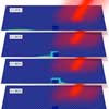
Theoretical Flow of Electrons

Theoretical flow of electrons in a two dimensional electron gas away from an electron source at the center. The same scattering that produces diffusion creates static branches of electron flow.Cover Article: Nature 410, 6825 (2001).
Theoretical Potential-Energy Surface For Mn Adsorption On GaAs(001)

Theoretical potential-energy surface for Mn adsorption on GaAs(001), calculated within density-functional theory. Phys. Rev. Lett. 89, 227201 (2002).
Three-Dimensional Rendering Of the Electric Field

Three-dimensional rendering of the electric field from numerical calculations in a random laser in which the yellow spheres represent the nanoparticles in a cylindrically symmetric gain medium. The electric field, where color and height indicate intensity, represents the steady-state solution of the Maxwell-Bloch system of equations. Hakan E. Türeci, A. Douglas Stone, Li Ge, Stefan Rotter, and Robert J. Tandy. "Ab initio self-consistent laser theory and random lasers, " Nonlinearity 22, C1-C18 (2009).
Transmission Electron

Transmission electron microscope image of chemically produced cobalt nanomagnets in the form of spheres and rods. The nanorods align with an applied magnetic field indicating that they are ferromagnetic.
Information for
About APS
The American Physical Society (APS) is a nonprofit membership organization working to advance the knowledge of physics.
© 2024 American Physical Society | Privacy Policy | Contact Us
1 Physics Ellipse, College Park, MD 20740-3844 | (301) 209-3200